|
Specific capabilities: micro/nano fabrication of photonic and related devices; fabrication of waveguides and photonic crystals; and MEMS.
|
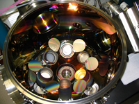
Inside RF/DC sputter coater, ANU |
The ANFF ACT node comprises facilities at the Australian National University and the University of Western Australia. These facilities are based on photonic / electronic materials growth, processing and fabrication of devices including micro electromechanical systems (MEMS). The node provides a range of capabilities and services for the micro/ nanofabrication of photonic and related devices as well as the fabrication of waveguides and photonic crystals. |
Optoelectronic devices such as semiconductor lasers, photodetectors and modulators are widely used for communications, data storage and medical applications. Further, photonic crystals, with their ability to confine light and guide and control its propagation, promise an entire suite of ultra-compact optical devices analogous to those of semiconductor electronics. Hence the node is internationally recognised for supporting both state-of-the-art research and proof of concept development for industry.
Facilities offered through ANFF include two metal organic chemical vapour deposition (MOCVD) reactors for the growth of III-V compound semiconductor multilayers based on: GaAs, AlGaAs, InGaAs, InP, InGaAsP, InAlGaAs, GaSb, InSb, InGaAsN. This capability is unique in Australia. The reactors enable the fabrication of nanowires, quantum dots, quantum wells, strained layers and devices.
The node also provides access to state-of-the-art fabrication facilities for optical MEMS and infrared sensor technology. Fabrication of micro electromechanical systems (MEMS) brings together modified semiconductor fabrication techniques, such as, molecular beam epitaxy (MBE), combined with micromachining to produce devices. Applications of the technology include automotive, defence, and communications.
The capability includes II-VI semiconductor growth by MBE and clean room micro / nano fabrication facilities (ICP/RIE, thin film deposition, etching, optical lithography, wire bonding and packaging) for the fabrication of nano / micro electromechanical systems (NEMS/MEMS).
Flagship facilities for the node include:
- Raith 150 electron beam lithography system for nanostructure fabrication
- RF /DC sputtering system for metal and dielectric multi-layer deposition
- Cluster tool for dry etching and deposition
- Dual beam focused ion beam
- Nano imprint lithography
Contact Details
Facility Manager: Dr Fouad Karouta
Email: fouad.karouta@anu.edu.au
Phone: +61 2 6125 7174
Node Director: Prof. Jagadish
Email: chennupati.jagadish@anu.edu.au
Phone: +61 2 6125 0363
Web: http://anff-act.anu.edu.au |
|
|
|
|
Instrumentation Available |
|
|
ANU
- Metal Organic Chemical Vapour Deposition Reactors
- Ion Implanters
- Rutherford Backscattering Spectrometry
- Pulsed Laser Deposition System
- High resolution x-ray diffractometers
- RF/DC sputtering system
- Raith 150 E-beam Lithography Facility
UWA
- Molecular Beam Epitaxy System
- Optical Lithography
- PECVD Deposition Systems
- E-beam and thermal evaporators
- Reactive Ion Etching
- Inductively Coupled Plasma Etching & Deposition
- Rapid Thermal Annealing
- Wire-Bonder
- I-V, C-V, DLTS, Hall Effect Measurement Systems
- Optical and MEMS Characterisation Facilities

|
|