|
 Specific capabilities: electron-beam lithography for large area structures, especially in nanoelectronics; ultra-high resolution EBL for small scale prototype devices; and semiconductor device prototyping. Specific capabilities: electron-beam lithography for large area structures, especially in nanoelectronics; ultra-high resolution EBL for small scale prototype devices; and semiconductor device prototyping.
Nanoelectronics is a critical enabling technology for a range of existing and developing industries. All modern-day computer processor chips are based on transistors with component sizes below 100 nanometers (500 times smaller than the width of a human hair). The development of new transistors, molecular electronics and other innovative device concepts relies on the ability to fabricate prototype devices on the nanoscale. Electron beam lithography (EBL) uses a highly focused beam of electrons to "write" such circuits at this tiny scale. Its flexibility allows for new concepts to be tested on a fast timescale and it is therefore a key tool in any nanoelectronics research laboratory.
The ANFF NSW node is hosted within the Semiconductor Nanofabrication Facility (SNF) at UNSW. Established in 1995, the SNF houses clean-room laboratories containing a comprehensive collection of micro-electronic and nano-electronic process equipment for fabricating an array of silicon (Si) and gallium arsenide (GaAs) devices. The laboratory currently supports ground-breaking research in silicon quantum computing, quantum electronic devices, medical radiation detectors and photovoltaics.
The node builds on its existing concentration of EBL systems and expertise in advanced nanoelectronics. During its 13 years of operation, SNF staff have developed significant knowledge and expertise in EBL process development and advanced lithography tool operation. The node will offer users the training required to fabricate complete devices, involving complex and advanced process flows.
The node provides a full device prototyping service including: device design and conception, photo-mask design, photo-mask fabrication (at the Bandwidth Foundry LINK) and process development.
Leading edge nano-photonic and nano-electronic applications demand high-resolution EBL over large areas (millimetres). The NCRIS program has enabled the purchase of a RAITH-150TWO EBL tool. This system allows fabrication of nanoscale structures (with feature sizes down to 20nm) over very large areas, up to 400 mm in size. Examples of structures that can be fabricated using this tool include holographic plates and photonic crystals. The RAITH-150TWO, together with a number of other essential microfabrication facilities, will come on-line in new purpose-built class 35 and class 350 clean-rooms in the third quarter of 2008.
NCRIS funding has also enabled the appointment for 3 additional technical staff with specific expertise in lithography, photo-mask design and semiconductor processing.
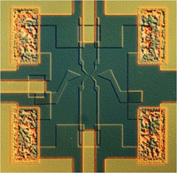
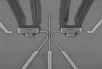
Image shows integrated silicon charge qubit prototype, incorporating dual single electron transistors for single charge sensing and nanoscale surface gates with feature sizes down to 20nm. Courtesy of ARC Centre of Excellence for Quantum Computer Technology and UNSW Semiconductor Nanofabrication Facility.
Contact Details
Node Director: Prof. Andrew Dzurak
Email: a.dzurak@unsw.edu.au
Phone: +61 2 9385 6311
Acting Facility Manager: Dr Linda Macks
Email: linda.macks@unsw.edu.au
Phone: +61 2 9385 7845
|